
tutorial_4b_split_keyboard_with_shift_registers.md 4.7KB
keybrd Tutorial 4b - split keyboard with shift registers
When you finish this tutorial you will be able to be able to modify a 2-matrix keybrd sketch to suite your own split keyboard design.
Overview of split keyboard with shift registers
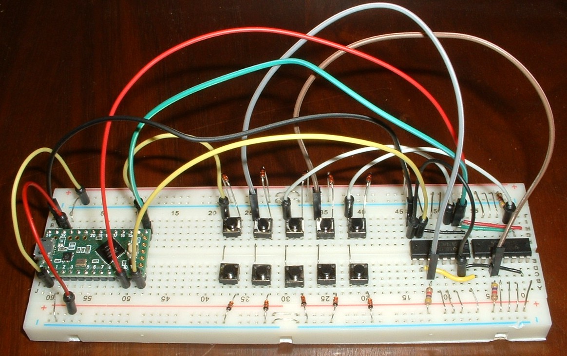
The breadboard in the following picture models a split keyboard.
The primary matrix on the left has one column, which is read by a microcontroller pin. The secondary matrix on the right has 4 columns, which are read by the shift register input pins. The primary and secondary matrices share the same rows, which are strobed by micro-controller pins. Both matrices are active low.
Building a split keyboard with shift registers
The breadboard keyboard modifies the basic breadboard keyboard described in tutorial_1_breadboard_keyboard.md
Add components to the breadboard as shown in the picture.
The shift register is a SN74HC165N. Details are in the SN74HC165N datasheet.
Each shift register has a small notch on one end to identify pin 1. In the picture, 1 pins are on the right end. Shift registers are chained together by colored wires that lay flat on the breadboard.
Each shift register has 8 parallel input pins, 4 on each side. The breadboard doesn’t have enough room for 16 columns; only 4 columns are connected to the shift registers. Every 4th input pin is connected to a matrix column and a pull-up resistor. Unused input pins are connected to power. The red bus strips power the pull up resistors and unused input pins.
A decoupling capacitor between the power and ground wires dampens noise coming in through those wires.
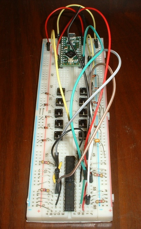
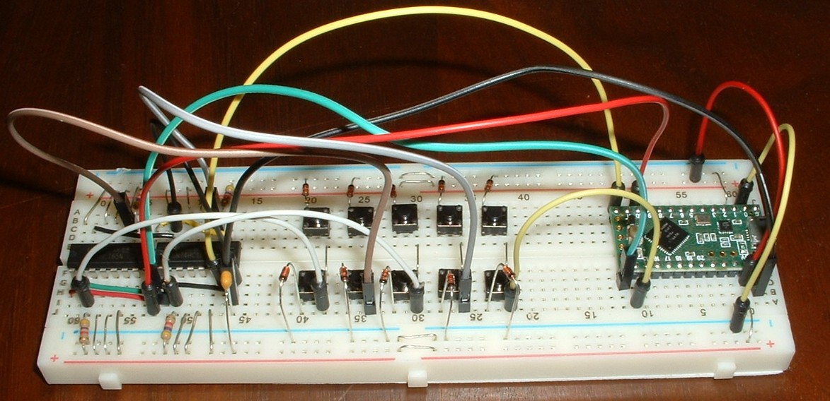
Blue bus strips are used for strobing rows
I apologize for not having a schematic. This table should help you figure out the pictures:
74HC165 left (upper half of breadboard)
NAME    PIN# I/O DESCRIPTION         DESTINATION     PIN#   CHAIN (wires flat on breadboard)
SH/LD   1    I   shift or load input Teensy LC CS0   10     red wire
CLK     2    I   clock input         Teensy LC SCK0  13     green wire
 D4     3    I   parallel input      pull-up resistor       red bus
 D5     4    I   parallel input      power                  red bus
 D6     5    I   parallel input      power                  red bus
 D7     6    I   parallel input      power                  red bus
/QH     7    O   ~serial output      Teensy LC MISO0 12
GND     8        ground              gnd                    black wire

74HC165 right (lower half of breadboard)
NAME    PIN# I/O DESCRIPTION         DESTINATION            CHAIN (wires flat on breadboard)
VCC     16       power pin           Teensy LC 3.3V         red bus
CLK INH 15   I   clock inhibit       gnd                    black wire
 D3     14   I   parallel input      power                  red bus
 D2     13   I   parallel input      power                  red bus
 D1     12   I   parallel input      power                  red bus
 D0     11   I   parallel input      pull-up resistor       red bus
SER     10   I   serial input        next QH                yellow wire
 QH      9   O   serial output       previous SER           yellow wire
Sketch for split keyboard with shift registers
keybrd_4b_split_keyboard_with_shift_registers.ino is a simple sketch with two shift registers. The sketch will run on the above breadboard keyboard. Annotations in the sketch explain the code.
Exercises
- Guess what happens if an unused input pin is not powered? Try it.

keybrd tutorial by Wolfram Volpi is licensed under a Creative Commons Attribution 4.0 International License.
Permissions beyond the scope of this license may be available at https://github.com/wolfv6/keybrd/issues/new.